AI Accelerator Cards Are Pushing Gap Filler Conductivity Past 10 W/mK — Here’s Why
The GPU in your AI training cluster isn’t the same component it was three years ago. The power it dissipates, the thermal management it requires, and the TIM it needs have all changed fundamentally. Here’s the engineering behind why 10 W/mK is becoming the floor for AI infrastructure thermal interfaces.
The POV
AI infrastructure is the fastest-moving demand signal in the thermal interface materials market right now. TC requirements are escalating faster than most TIM product roadmaps anticipated. If you’re specifying TIM2 for GPU clusters today, design for 10 W/mK minimum — and build in a qualification path for 12–15 W/mK grades as they mature.
The Power Density Problem — Why AI GPUs Changed the Thermal Equation
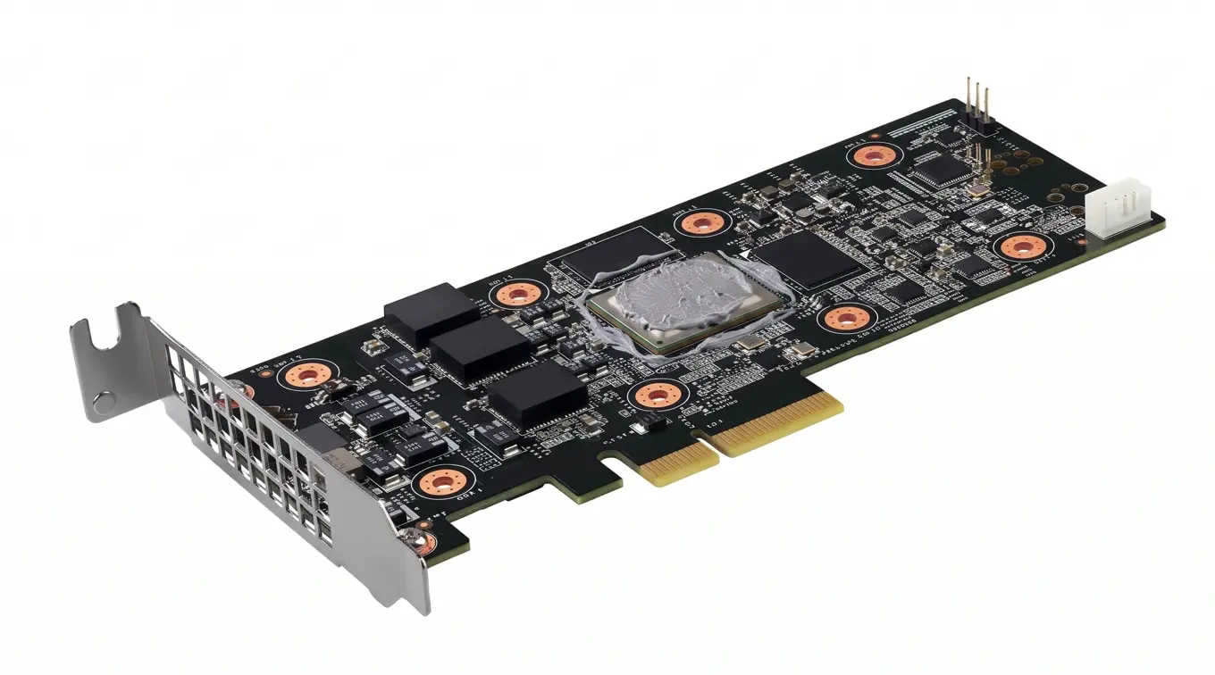
NVIDIA’s H100 GPU dissipates up to 700W in its SXM5 form factor — and its successors push past that. Power density on the silicon die has roughly doubled in three GPU generations. The compute performance scales with power. The heat follows.
This isn’t an accident of design. It’s the physics of running large matrix operations on massive parallel architectures at clock speeds that extract maximum throughput per watt of manufacturing process. The compute performance scales with power. The heat follows. The thermal management system has no choice but to keep up.
Where the Heat Actually Goes — and Where TIM2 Sits
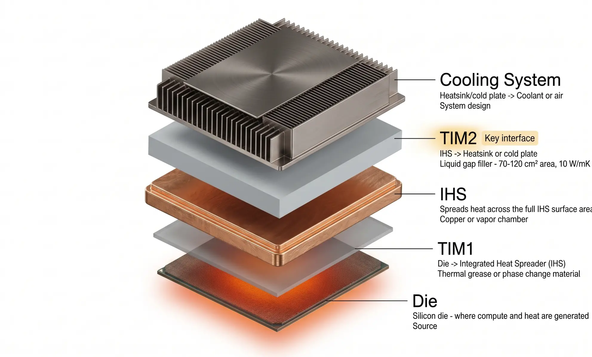
In an AI accelerator card, the primary thermal path has four interfaces. TIM2 — the gap filler between the IHS and the cooling system — is where liquid gap filler is increasingly relevant, and where the 10 W/mK requirement originates.
AI Accelerator Thermal Path — Interface by Interface
| Interface | Description | TIM Type |
|---|---|---|
| Die | Silicon die — where compute and heat are generated | Source |
| TIM1 | Die → Integrated Heat Spreader (IHS) | Thermal grease or phase change material |
| IHS | Spreads heat across the full IHS surface area | Copper or vapor chamber |
| TIM2 Key interface | IHS → Heatsink or cold plate | Liquid gap filler — 70–120 cm² area, 10 W/mK target |
| Cooling system | Heatsink/cold plate → Coolant or air | System design |
Why TIM2 Is the Critical Interface for Gap Filler
Large Interface Area
70–120 cm² for a full-size GPU IHS — any thermal resistance at this interface is multiplied across a large area, making even small TR improvements meaningful
Surface Non-Flatness
IHS bow and heatsink surface variation create a non-uniform gap that fixed-thickness gap pads cannot conform to — liquid gap filler self-levels to fill actual topography
High Power Flux
700W+ across 100 cm² = 7 W/cm² average power density at TIM2 — with local hotspots significantly higher where compute blocks concentrate power
700W Across 100 cm² — What TC Grade Actually Means for Junction Temperature
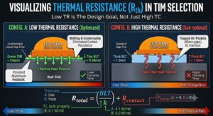
At 700W across a 100 cm² IHS with a 0.3 mm gap, the TC grade of your TIM2 material directly determines how much of your junction temperature budget is consumed at this one interface.
| Parameter | Standard Gap Filler — 4.1 W/mK | TIA2101GF — 10.1 W/mK |
|---|---|---|
| Power | 700 W | 700 W |
| Interface area | 100 cm² = 10,000 mm² | 100 cm² = 10,000 mm² |
| Gap / BLT | 0.3 mm = 300 µm | 0.3 mm = 300 µm |
| TR at BLT | 73 mm²K/W | 30 mm²K/W |
| ΔT across TIM2 | 5.1°C | 2.1°C 3.0°C lower |
| Impact on boost clock | Higher junction temp → lower sustained boost frequency | Lower junction temp → higher sustained boost, more tokens/sec Performance advantage |
3°C at this power level is not trivial. GPU junction temperature directly affects boost clock frequency — a cooler GPU runs at higher sustained clock, delivering more tokens per second in inference or more iterations per day in training. The performance-per-dollar of an AI cluster is partially a function of how well the TIM2 interface is managed. At $15,000–30,000 per GPU card, 3°C of thermal headroom is an operating economics question, not just a thermal engineering one.
Why 10 W/mK Is Becoming the Baseline for AI Infrastructure TIM2
Three years ago, 4–6 W/mK was considered high-performance for server applications. The AI infrastructure build-out has changed that reference point fundamentally — driven by four specific requirements from data center operators.
TC ≥ 10 W/mK for Boost Frequency Threshold
Data center operators require TC ≥ 10 W/mK at the IHS-to-cold-plate interface to maintain junction temperatures within boost frequency thresholds — where the GPU delivers its rated inference throughput
Stable TR Across Thermal Cycles
GPU cards cycle on and off with workload in inference clusters — significant thermal fatigue stress on TIM2. Stable thermal resistance through thousands of power cycles is a reliability specification, not a preference
Low Volatile Siloxane Content
In sealed rack environments, siloxane contamination of optical transceivers and relay-controlled power distribution is a data center operations concern. LV D4–D10 specification is becoming a data center procurement requirement
Reworkability — $15K–30K Cards Must Be Serviceable
A TIM that bonds irreversibly is a maintenance liability at GPU card price points. Reworkable silicone elastomers that peel cleanly without adhesive residue are required for field serviceability of high-value compute assets
12–15 W/mK — What’s Coming Next
Experimental pre-cured gap filler grades are now in active development for next-generation AI accelerator applications — targeting power densities that exceed what current 10 W/mK grades can manage at acceptable junction temperatures.
15.7 W/mK (ASTM D5470) — experimental pre-cured grade for next-generation AI accelerator TIM2 interfaces. Targeting sustained power densities above 30 W/cm² in liquid-cooled GPU and accelerator ASIC packages.
Pre-cured
Development stage
15.0 W/mK (ASTM D5470) — experimental grade in active development for liquid-cooled accelerator platforms. Addresses the formulation challenge of achieving 15 W/mK while maintaining low modulus to protect silicon substrates.
Pre-cured
Development stage
The formulation challenge at 15 W/mK: High-TC grades require high filler loading, which increases stiffness and raises risk of IHS stress concentration on the silicon substrate. The engineering challenge is achieving 15 W/mK while keeping Type E hardness low enough to protect the die. It’s a materials engineering problem — not just a conductivity optimization — which is why development timelines are measured in years, not months.
Production-Ready Grade for AI Accelerator TIM2 — TIA2101GF at 10.1 W/mK
While 12–15 W/mK grades are in development, TIA2101GF at 10.1 W/mK is the production-ready grade for AI server GPU TIM2 applications today — delivering the 3°C junction temperature advantage over standard 4.1 W/mK gap filler at 700W power levels.
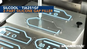
10.1 W/mK liquid dispensed silicone gap filler. 2-part curing system, 1:1 mix ratio. Minimum BLT 280 µm. The benchmark production grade for AI accelerator IHS-to-cold-plate (TIM2) interfaces and high power density EV battery and telecom applications.
280 µm min BLT
Reworkable
Low LV siloxane
2.1°C ΔT at 700W / 100 cm²
Frequently Asked Questions
AI GPU accelerators such as NVIDIA H100 SXM5 dissipate up to 700W — roughly double the power density of previous GPU generations. At 700W across a 100 cm² IHS interface, a standard 4.1 W/mK gap filler creates 5.1°C temperature drop at TIM2. TIA2101GF at 10.1 W/mK reduces this to 2.1°C — a 3°C improvement that translates directly to higher sustained GPU boost clock frequency and more tokens per second in inference workloads.
TIM2 is the thermal interface material between the Integrated Heat Spreader (IHS) and the heatsink or cold plate — distinct from TIM1 (die-to-IHS). TIM2 interfaces are typically 70–120 cm² and face IHS bow and heatsink surface variation requiring a conformable material. At 700W+ power levels, the TC grade of TIM2 directly determines junction temperature and sustained boost clock performance — making it a first-order design specification, not a commodity procurement decision.
Data center operators requiring thermal management for next-generation GPU clusters are specifying TC ≥ 10 W/mK at the IHS-to-cold-plate interface. TIA2101GF at 10.1 W/mK is the current production-ready grade. Experimental grades at 15.0–15.7 W/mK (KXE14-1140, KXE13-1149) are in active development for next-generation platforms targeting sustained power densities above 30 W/cm².
AI GPU cards cost $15,000–30,000 each. A TIM that bonds irreversibly creates a maintenance liability — the card cannot be serviced without destructive TIM removal that risks component damage. Reworkable silicone elastomer gap fillers peel cleanly from IHS and heatsink surfaces without adhesive residue, enabling card-level service and re-deployment. At data center scale, the ability to service and redeploy compute assets without full card replacement has significant economic value.
Achieving 15 W/mK requires very high filler loading, which increases elastic modulus. Higher modulus raises the risk of mechanical stress concentration at the IHS-silicon substrate boundary during thermal cycling — a failure mode that can damage the substrate. The formulation challenge is achieving 15 W/mK while keeping Type E hardness low enough to protect the silicon die. This is a materials engineering optimization — not just conductivity maximization — which is why development timelines for these grades are measured in years.
In sealed rack environments, volatile cyclic siloxanes (D4–D10) outgassing from silicone materials can contaminate optical transceivers and relay-controlled power distribution equipment. Data center operators increasingly specify maximum LV siloxane content — typically <100 ppm — for materials inside server and switching racks. This is becoming a standard procurement specification for gap fillers in AI infrastructure, particularly in high-density rack configurations where the enclosed environment concentrates outgassing.
Design for 10 W/mK Now — Build the Path to 15 W/mK
Specify TIA2101GF at 10.1 W/mK for current AI GPU TIM2 interfaces. Begin qualification planning for 12–15 W/mK grades for next-generation platforms. The TC requirements are escalating faster than product roadmaps anticipated — and the junction temperature headroom saved today is the performance margin that keeps AI clusters running at boost frequency under sustained workload.