Telecom Base Station Thermal Management: RF PCB to Heatsink in 3 Steps
Base station hardware runs hotter than it used to. 5G Radio Unit power densities have increased significantly over 4G, and the thermal path from RF components to the enclosure exterior is becoming a design bottleneck — with fewer options to address it once the layout is fixed.
The One Variable You Can Still Control
Once component selection and PCB layout are fixed, the thermal interface material at each boundary in the thermal path is one of the few design variables an engineer can actually optimize. In outdoor-passive-cooled 5G RU designs, getting the TIM right is not optional — it is the primary thermal lever.
Why 5G Changed the Thermal Equation for Base Station Design
The thermal challenge in 4G base stations was concentrated and manageable. 5G Massive MIMO Radio Units replaced it with a fundamentally different power distribution problem that conventional thermal management approaches cannot address the same way.
Passive (conduction/convection) cooling means the thermal path from device junction to enclosure exterior must carry more heat with no active cooling assistance — making every interface in that path a first-order design decision, not an afterthought.
The 5G RU Thermal Path — Where TIM Makes the Most Impact
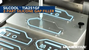
A typical 5G Radio Unit thermal path has three interfaces. Liquid gap filler has the most impact at TIM 2 — the PCB assembly-to-enclosure interface — because this is where gap variation, surface non-flatness, and environmental reliability requirements converge.
5G RU Thermal Path — Interface by Interface
| Interface | Description | Typical TIM |
|---|---|---|
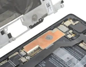
| TIM 1 | RF PCB (PA, transceiver, BBU) → heatspreader or cold plate | Thermal grease, phase change film, or thin gap filler |
| TIM 2 Highest impact | Heatspreader / PCB assembly → enclosure wall or thermal frame | Liquid dispensed gap filler — non-flat interfaces, variable gaps, vibration |
| TIM 3 | Enclosure wall → fins / enclosure surface → ambient | Enclosure design — not a TIM decision |
Why TIM 2 Is Where Liquid Gap Filler Has the Most Impact
Non-Flat Interface Topology
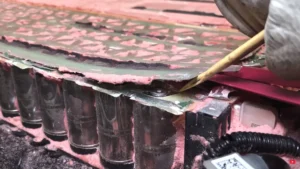
Populated PCBs have component height variation across the board — the heatspreader or chassis back-wall is not perfectly parallel to the PCB surface
Significant and Variable Gap
Gap typically ranges from 0.5–2 mm depending on component height variation — requires a TIM that self-levels to fill variable-depth gaps, not a fixed-thickness die-cut pad
Vibration and Cycling Resistance
Outdoor base stations experience wind-induced vibration and thermal cycling from -40°C to +85°C — gap pads can lose contact or creep; cured silicone elastomers absorb vibration without delaminating
Characterize Your Interface Gap and Topology
Before selecting a TIM grade, measure the actual gap at your thermal interface. Gap varies across the PCB because component heights vary — your TIM must fill the maximum gap while maintaining adequate contact at the minimum gap location.
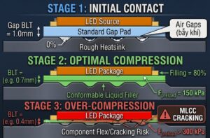
Profile measurement finding: Measurements across populated 5G RU boards typically show 0.3–1.5 mm variation in gap depth across the interface. A die-cut gap pad specified at a fixed thickness cannot accommodate this variation — it either bottoms out at thin locations or leaves air gaps at thick locations. Liquid gap filler self-levels to fill whatever gap exists; BLT is set by the assembly closure pressure, not the material’s pre-specified thickness.
Grade Selection by Interface Gap Range
4.1 W/mK thermally conductive silicone gap filler. Minimum BLT 120 µm. Suitable for 0.1–2 mm interface gaps. Covers most 5G RU PCB-to-chassis applications at mid power density.
120 µm min BLT
0.1–2 mm gap range
Mid-density RU
10.1 W/mK ultra-high thermal conductivity silicone gap filler. Minimum BLT 280 µm. For high power density Radio Units and AAU designs where junction temperature budget is tight.
280 µm min BLT
High power density
AAU applications
Select TC Grade Based on Thermal Budget
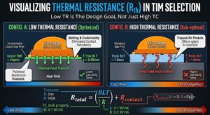
The thermal resistance calculation at the TIM interface is straightforward. Run this calculation for your actual power dissipation, interface area, and target BLT — then select the grade that keeps ΔT within your thermal budget.
Thermal Resistance Formula
ΔT across TIM = Q × (BLT ÷ TC ÷ A)
Where: Q = heat flux (W) · BLT = bondline thickness (m) · TC = thermal conductivity (W/mK) · A = interface area (m²)
Worked example — 5G RU: 50 W dissipated across a 100 cm² interface at 1 mm BLT:
| Grade | TIA241GF — 4.1 W/mK | TIA2101GF — 10.1 W/mK |
|---|---|---|
| Calculation | 50 × (0.001 ÷ 4.1 ÷ 0.01) | 50 × (0.001 ÷ 10.1 ÷ 0.01) |
| ΔT across TIM | 1.22°C | 0.50°C 0.72°C lower |
| Thermal resistance | 24.4 mm²K/W | 9.9 mm²K/W 2.5× lower |
| Best fit | Mid-density RU — standard 5G radio units | High power density RU, AAU, tight junction temp budget |
In telecom applications, a 0.7°C improvement at the TIM level directly translates to extended component life — or headroom for power increase in the next product generation. At scale across a network deployment, this margin has real operational value.
Validate for Vibration and Outdoor Environmental Requirements
Outdoor-rated base station TIM must survive a qualification envelope that indoor electronics TIM is never tested against. Silicone gap fillers have inherent advantages in this environment — but verify explicitly against your standard before specifying.
Thermal Cycling
-40°C to +85°C per ETSI EN 300 019 or equivalent. Silicone maintains elasticity across -55°C to 200°C — inherently suited to outdoor thermal cycling without cracking or delamination
Vibration
IEC 60068-2-6 sinusoidal or IEC 60068-2-64 random vibration. Cured silicone elastomer absorbs vibration energy rather than transmitting it — gap pads can lose contact under repeated vibration cycles
Damp Heat
85°C / 85% RH for 1000 hours. TIA2101GF reliability data shows stable TC and hardness after 1000h at 85°C/85%RH aging — published reliability data is the qualification baseline
High-Temperature Aging
TIA2101GF shows stable TC and hardness after 1000h at 150°C aging — critical for RU designs where internal temperatures can significantly exceed ambient in full sun outdoor deployment
Verification requirement: For designs requiring explicit vibration resistance certification, verify the specific grade against your test standard — not all gap filler formulations have been qualified to ETSI/IEC profiles. Request reliability aging data from your supplier that matches your qualification standard before specifying the grade into production.
Grade Selection Summary for 5G RU and AAU Applications
| Design Requirement | TIA241GF — 4.1 W/mK | TIA2101GF — 10.1 W/mK |
|---|---|---|
| Thermal conductivity | 4.1 W/mK | 10.1 W/mK 2.5× higher |
| Minimum BLT | 120 µm | 280 µm |
| Interface gap range | 0.1–2 mm | 0.3–2 mm |
| Target application | Standard 5G RU, mid-density macro cells | High power density RU, AAU, tight junction temp budget Recommended |
| Thermal cycling reliability | -40°C to +85°C stable | Qualified — stable TC & hardness after 1000h @ 150°C and 85°C/85%RH |
| Outdoor passive cooling | Suitable | Suitable More headroom |
| Interface gap variation | Self-levels across full gap range | Self-levels across full gap range |
| Vibration resistance | Cured elastomer — absorbs vibration | Cured elastomer — absorbs vibration |
| Reworkable | ✅ Yes | ✅ Yes |
| Automatable dispensing | ✅ Yes | ✅ Yes |
Frequently Asked Questions
Liquid dispensed silicone gap fillers are recommended for 5G RU PCB-to-chassis interfaces. TIA241GF at 4.1 W/mK covers most mid-density 5G Radio Unit applications. TIA2101GF at 10.1 W/mK is recommended for high power density RU and AAU designs where junction temperature budget is tight. Both products self-level to fill variable-depth gaps caused by component height variation — a fundamental advantage over fixed-thickness die-cut gap pads in non-flat interfaces.
5G Massive MIMO Radio Units distribute heat across arrays of many smaller amplifiers across multiple frequency bands — replacing the 4G concentrated single-amplifier challenge with distributed higher-density heat across the entire RF PCB. Simultaneously, 5G RU enclosures are increasingly designed for outdoor passive cooling to meet IP66/IP67 requirements — the thermal path from device junction to enclosure exterior must carry more heat with no active cooling assistance.
Three advantages: (1) Self-leveling fill — populated PCBs show 0.3–1.5 mm gap variation due to component height differences; liquid gap filler fills whatever gap exists while fixed-thickness pads cannot accommodate this variation; (2) Lower thermal resistance — TIA241GF at 4.1 W/mK with 120 µm minimum BLT achieves significantly lower resistance than gap pads at equivalent gaps; (3) Vibration and thermal cycle resistance — cured silicone elastomers absorb vibration and maintain contact through -40°C to +85°C cycling without the contact loss or creep observed with gap pads.
For a 5G RU dissipating 50W across a 100 cm² interface at 1 mm BLT: TIA241GF at 4.1 W/mK gives ΔT = 1.22°C across the TIM (24.4 mm²K/W). TIA2101GF at 10.1 W/mK gives ΔT = 0.50°C (9.9 mm²K/W). The 0.72°C improvement translates to extended component life or headroom for power increase in next-generation RU designs.
Outdoor-rated base station TIM must typically survive: thermal cycling -40°C to +85°C per ETSI EN 300 019; vibration per IEC 60068-2-6 (sinusoidal) or IEC 60068-2-64 (random); and damp heat 85°C/85%RH for 1000 hours. TIA2101GF has published reliability data showing stable TC and hardness after 1000h at both 150°C and 85°C/85%RH aging. Verify the specific grade against your qualification standard — not all gap filler formulations are qualified to ETSI/IEC profiles.
TIA241GF — minimum BLT 120 µm, gap range 0.1–2 mm. TIA2101GF — minimum BLT 280 µm, gap range 0.3–2 mm. Both products self-level to fill the actual assembly gap — BLT is set by closure pressure rather than a fixed material thickness, which is a fundamental advantage over die-cut gap pads that must be specified at a single thickness.
3-Step Selection Summary
Step 1: Profile your interface gap — measure actual gap variation across the populated PCB. Step 2: Calculate ΔT across the TIM using your actual Q, BLT, and interface area — select TIA241GF for mid-density or TIA2101GF for high power density. Step 3: Verify the grade against your outdoor reliability standard — thermal cycling, vibration, and damp heat qualification.